Why MOSFET and IGBT characteristics are different? – FAST TURN CHIP
Fets were invented at Bell LABS in the 1950s, and today you have billions of them in your COMPUTER CPU. IGBT is the high-power device invented by Prof. Baliga, who is counting on it to win the dynamite prize. These are the landmarks of the semiconductor industry, and they are used everywhere today, but no one really looks at the differences and the principles.
As we all know, FETs including MOSFET, JFET and so on can be used in higher frequency applications, and their characteristics are more similar to a resistor, namely the on-resistor. The transistor type of power semiconductor, such as IGBT, the relative frequency is lower, the current is higher, but there is a conduction forward voltage. Why is this happening? So let’s analyze it. The following is only my personal understanding, welcome to discuss.
First, review the basics
We know that intrinsic semiconductors are non-conductive, just like pure water is not conductive, so if you want it to be conductive, you mix it with impurities. To make water conduct electricity, salt is added to produce ions. To make semiconductors conduct electricity, trivalent or pentavalent elements are added to form holes or electrons.
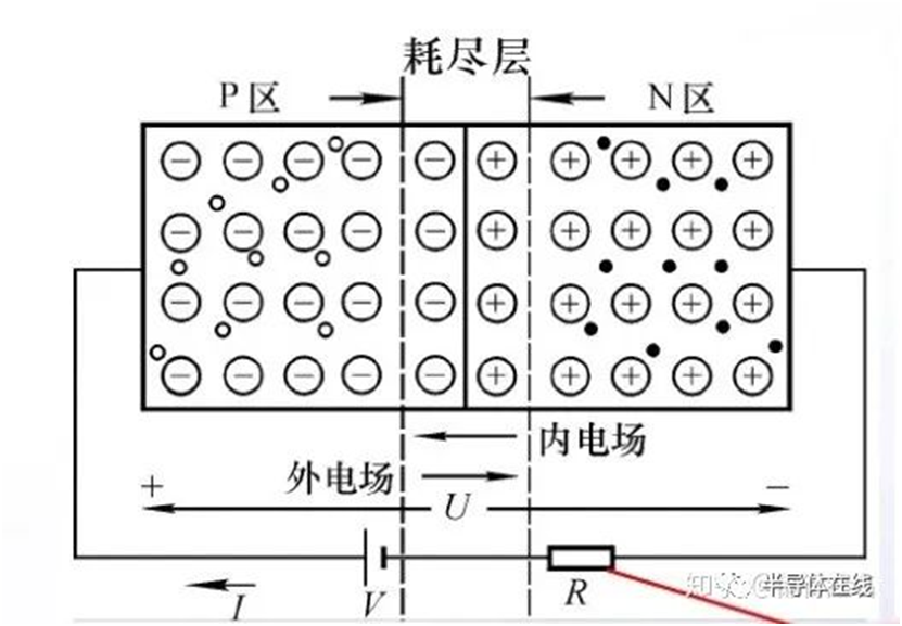
If you put p-type and N-type semiconductors together, you form a PN junction. Because of the p-type semiconductor hole, n-type multi-electron, the way of heaven damage and complement, so, the electron will diffuse from the N side to the P side, this is called diffusion. And then there’s an electric field, N to P, that’s going to pull the electron back, and that’s called drift. The two have reached equilibrium to some extent, and the small area with electric field formed in the middle is called the Depletion zone Depletion region. Because the electrons in the depletion layer are already in the hole, like the ions in water, the depletion layer does not conduct electricity.
In order for the PN junction to conduct, it is positively deflated, cancelling out the electric field in the depletion layer, so that electrons can flow happily again, and diffusion is successfully unlocked. This split lock voltage is the threshold voltage of the diode. However, due to the positive and negative bias of this junction, there will be a certain charging effect, which can be equivalent to a nonlinear capacitor. Therefore, the device with PN junction has the highest operating frequency, and no higher than that, it cannot block the voltage. This is easy to understand because capacitors cannot block AC voltage.
With the basic knowledge replenished, let’s take a look at the structure of the field effect tube.
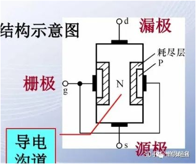
1. Below is the structure of an N-channel JFET. It already has a whole n-type semiconductor in the middle, so when you don’t apply any voltage, it’s on. What if you want it to shut down? So I’m going to apply a negative voltage between the gate and the source, and this depletion layer is going to increase, and we know that the depletion layer has no free electron holes, so it’s no longer conducting. It’s like when you pinch your nose slowly until the sides are together and you can’t breathe. This is why a JFET is a common device and is used in many solid state circuit breakers.
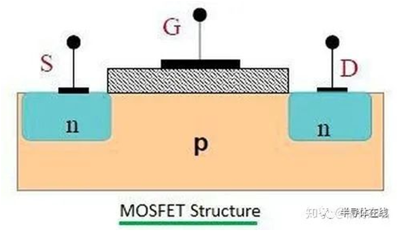
2. How to achieve normally closed MOSFET? This is a simple planar N-channel MOSFET structure. It should be noted that the figure shows a horizontal MOSFET, which is usually used in low-power devices such as CMOS. However, in order to increase the voltage, the power MOSFET usually adopts a vertical structure, which is commonly referred to as VDMOS. As you can see, it can’t conduct because it’s blocked by the PN junction on the right. How do you make it work?
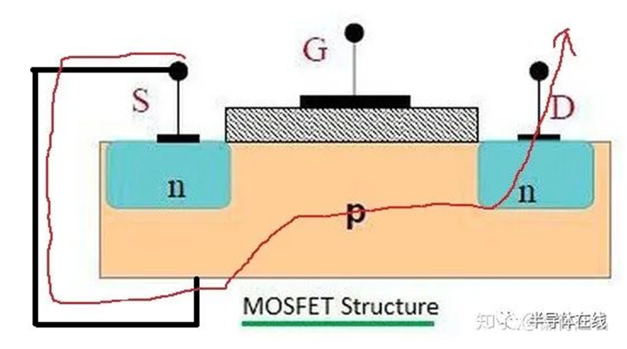
A forward voltage is applied between G and S, and at the same time, the bottom (base) of the P-type semiconductor is connected to the S pole. Since there is an insulating layer made of silicon dioxide between G and P, adding a positive charge to G will induce a layer of electrons on the semiconductor of P, and this layer of electrons will form an N-type conductive channel. The trick here is that, in general, the thicker the layer of silica (GOX), the less likely the gate is to break down and the better the quality of the pipe. The D and S poles also rely on electrons to conduct electricity, so the entire MOSFET is on. We all know that the higher the Vgs, the lower the resistance, and here’s why: The higher the Vgs, the more electrons are induced.
3. Because MOSFET and JFET conduct electricity without a PN junction between them, they act like a resistor. However, for the transistor type, it is two reverse PN junctions, so when conducting, the internal electric field of a PN junction must be overcome first. Therefore, generally IGBT and BJT will have a certain forward voltage. As previously analyzed, IGBT and BJT frequencies are generally not as high as those of field-effect devices due to the presence of PN junction capacitance.
4. Why is the MOSFET behaving like a diode after reverse connection? As shown in the figure, it is very clear that a positive biased PN junction is formed naturally, which is the bulk diode. In the same way, when you add positive Vgs, after conducting channel formation, even if the wizard, current will take voltage lower conductive channel pathway, therefore, against the wizard sense with Vgs allows conduction voltage drop is reduced, which is why LLC, category contains phase-shift full bridge rectifier topology and totem poles PFC, hope can do synchronous rectifier efficiency.
Let’s look at the structure of IGBT
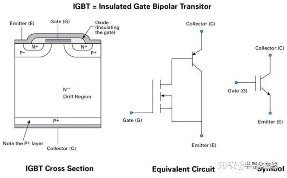
Its working principle can be analyzed according to the above method. As can be seen from the equivalence diagram, IGBT has a triode series MOSFET. Therefore, the PN junction of the triode brings forward voltage, and the junction capacitance also brings greater switching loss. However, unlike MOSFET, which conducts electricity only in the channel part, IGBT has a larger conduction area and can conduct more current. Therefore, IGBT is usually used in high power and low frequency occasions. In addition, when the reverse voltage, this part of the voltage is added to the PNP, so IGBT does not come with a body diode, and generally cannot withstand a higher reverse voltage, need to be connected to an anti-parallel diode outside to enhance the anti-guide ability.
About Electronic components distributor FAST TURN CHIP
FAST TURN CHIP is a B2B electronic contract manufacturer, with a number of electronic components procurement points. We can find and purchase hybrid electronic components and ics at competitive prices to meet customer needs. No matter what components you want, no matter how many, you can buy from Cocreate At a reasonable price and with traceable quality.
TLV320ADC5140IRTWR
PCA9641BSHP
NCP81239MNTXG
BQ25611DRTWR
PSMN0R7-25 yldx
For quotation please contact: Miss Huang 15018735409
Company website: https://fastturnchip.cn/

